

CHIPS: A Critical Moment for Electronics (Part 1).
Part 1: What are “chips,” and why are they always in the news?
A “chip” is an informal industry name for a combination of electronic circuits made up of many materials, including silicon, that process electricity and move information. Chips face a critical moment in history for the United States. The Biden Administration has begun an expansive effort on multiple fronts to change the way semiconductor research, development, manufacturing, and distribution takes place in the US. Over the last fifty years, offshoring to decrease cost and globalization has caused most manufacturing to take place in Taiwan and outside the US. The CHIPS and Science Act, passed in 2022, aims to bend that trend curve to ensure the US maintains semiconductor leadership.
Before we understand what the CHIPS Act is tryling to solve, it is important to understand the complexity of the technology at a fundamental level. Read on for an explainer on how we arrived here. Part 2 talks more about what happens next in the regulatory landscape and opportunities for businesses.
There are two key elements to the story: First, the ubiquitous presence of semiconductor chips in all of our electronics and, second, the unbelievably complex ecosystem involved in chip design, creation, and distribution.
Ubiquity: Essentially, if the object can be powered on, it probably has a semiconductor chip: From alarm clocks, to appliances, to cell phones, to network security systems of our most important critical infrastructure, to our national security defense systems. Our entire modern economy depends on a robust and dependable constant stream of semiconductor chips. As the technology evolves, the chips can process more information in smaller spaces, leading to advances in computing power (and, in turn, controlling information storage and distribution). Thus, controlling chips essentially controls everything.
Complex Ecosystem & Technology: The complexity of stakeholders in the semiconductor ecosystem comes from how small and sophisticated the semiconductor chip is. Figure 1 below shows a cross section of a chip. At its most basic function, the semiconductor chip is moving electricity through several dozen layers of material, each individually designed using sophisticated tools. Each layer has a mix of materials and chemicals. Silicon is a key material and extremely helpful because, depending on what is mixed with the silicon, it can be a move or slow the flow of electricity. The designs of each layer add up to intentionally microscopic (or nanoscopic) paths for the electricity to flow and reach a transistor, which creates all the ones (when electricity passes through) and a zero (when it does not).
Amazingly, the transistor operates at a scale of 2-10 nanometers (a piece of paper is 100,000nm thick) (Source). The A17 chip in the iPhone 15 Pro has approximately nineteen billion transistors (Source).
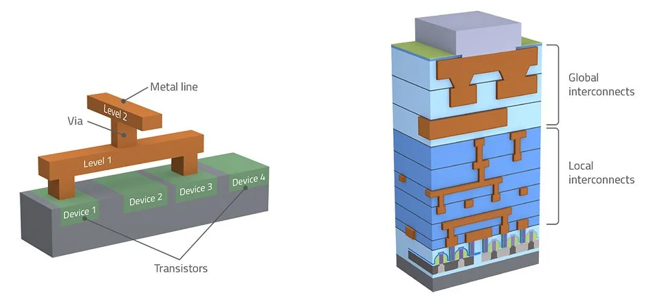
Fig. 1: Cross-section of semiconductor chip (brown is copper, blue is other non-conductive chemical materials (dielectric) (Source).
Technology this sophisticated is extremely expensive to manufacture at scale. As an example, ASML, a Dutch company that makes tools to “carve” the circuitry in each layer in a process called lithography using extreme ultraviolet light. ASML recently announce the next generation tool will cost approximately $300 million (Source). On top of that, this is one tool of several dozen needed in a fabrication manufacturing facility (“Fab”).
The lifecycle of chip development is long and deep, from basic research and experimentation at the outset to manufacturing a proven capability at scale. The number of players and prospective creates an incredible challenge because is no single owner of the overall process. Usually, universities are in the early stages of the process and for-profit manufacturers and tech companies are at the end of the lifecycle. There are a host of companies, government agencies and labs, non-profits, and for-profits in between that advance and innovate on a capability throughout the process.
It is a safe bet that the top thought leaders in each organization have a PhD and made it his/her/their life’s work focusing on a hyper-specific part of the process. It is very difficult to find someone with the education and training to understand every part of the chip design and functionality. With this level of specialization and fixed universe of required parties, industry stakeholders often must collaborate to advance chip capability, albeit sometimes with competing interests and perspectives.
Add to this the geographically diverse location of key players in the industry around the world. Research and development happens in the United States, Europe, South Korea, Japan, and other key allied nations. As a result of price demands, most manufacturing of semiconductor chips is in Taiwan. China is making a strong effort to take the lead in controlling the industry.
With the stage set on what is happening and who is in the game, read on to Part 2 for additional information about recent legislation and mobilization efforts to keep the US in the lead in the semiconductor industry.
Disclaimers: The above post does not qualify as legal advice.
Additionally, contacting Clock Speed G.C. does not create an attorney-client relationship. Please review our Disclaimer for additional information.